

Coulomb Blockade
Coulomb blockade suppresses sequential electron transfer through a small island because changing its integer charge costs energy. A gate changes that cost; a source–drain bias makes some transfers energetically favorable. The resulting conductance peaks and bias thresholds let us measure charging energies and capacitance ratios.
We begin with a normal-metal island, opaque tunnel barriers and a dense single-particle spectrum. This orthodox model treats each transfer perturbatively and describes the island by its charge-state probabilities. Discrete dot levels, strong tunneling, superconductivity and an energy-exchanging environment require extensions.
Required background. Chemical potential explains addition energies and reservoir comparisons; quantum dots introduces confinement and charging; mesoscopic transport develops sequential rates and charge-state probabilities.
Integer charge and charging energy
Section titled “Integer charge and charging energy”The island has excess electrons and charge . Let be its capacitance to electrode at electrical potential , including source, drain, gate and any stray conductors. Define
is a static charge offset. At fixed electrode voltages, the charge-dependent electrostatic potential, including the capacitor response to voltage sources, is
up to an -independent term. Some authors call the charging energy; compare the defining equation before comparing numbers. The orthodox description and its experimental realization are discussed by Averin and Likharev (1986) and Fulton and Dolan (1987).
The island’s next addition threshold is a difference of parabolas:
At zero lead bias, neighboring charge states are degenerate at . At an integer , either adding or removing one electron costs . The spacing between successive addition thresholds is instead : it is the second difference . These are distinct energies.
Changing only the gate gives the ideal period . A change shifts the same pattern by ; slowly moving charges therefore cause offset drift.
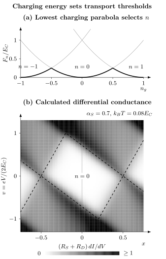
Top: the lowest parabola selects the stable charge at zero bias. Bottom: differential conductance from the normal-metal sequential-tunneling rates below, with equal junction resistances, , and . The grayscale saturates at , so black also represents values above this limit. Here , the drain is grounded, and . Dashed lines are zero-temperature thresholds. The diamond tips occur at and ; the vertical cut at meets the edges earlier, at . Thermal rounding softens the edges without changing the underlying electrostatic construction.
The figure uses the full charge-state rate equation, with charges ; enlarging this range leaves the displayed map unchanged. It does not include cotunneling or an environmental energy-exchange spectrum.
The energy change of one tunneling event
Section titled “The energy change of one tunneling event”Electrical potential and electron electrochemical potential have opposite signs: take relative to a common reference. If an electron enters the island from lead , the lead loses an electron as the island gains one. The total free-energy change is therefore
For an electron leaving an -electron island,
The reverse of is , so . Keeping the charge index is essential. A positive is uphill; a negative one releases energy.
For a normal-metal junction with resistance , constant densities of states and the same electron temperature on both sides, the orthodox rate is
Its numerator and denominator have the same sign. The expression counts occupied initial states and empty final states; equivalently its energy factor is . This continuum phase space distinguishes a metallic junction from a single discrete dot level, whose rate involves a Fermi factor rather than this energy integral (Ingold and Nazarov, 1992; Beenakker, 1991).
Three limits help check the formula:
It also obeys local detailed balance,
A finite rate at degeneracy does not mean equilibrium current: forward and backward events balance.
When are these rates reliable?
Section titled “When are these rates reliable?”For an opaque normal junction, each transmission eigenvalue is small and its total dimensionless conductance should satisfy , where . This controls quantum charge fluctuations. Separately, resolving a deep blockade valley requires , while using thermally broadened sequential rates requires lifetime broadening . These are controlled-regime conditions, not sharp boundaries; near a charge degeneracy the thermal populations are deliberately shared.
For example, an energy-releasing event with through has a low-temperature rate about . Its energy width is only . Always distinguish a rate from an energy broadening.
Coulomb diamonds from four inequalities
Section titled “Coulomb diamonds from four inequalities”Ground the drain and bias the source: , . Then and . Write and ; any other electrode potentials are held fixed. For one island transition,
An -electron state blocks sequential transfer at zero temperature if adding from either lead and removing to either lead are all uphill. Compactly,
Equality gives an edge. Drain alignment, , and source alignment, , have slopes
The denominator in includes drain, gate and stray capacitances. Swapping the biased lead changes the formulas. Reversing the plotted bias reverses both slope signs.
Tip height versus a vertical cut
Section titled “Tip height versus a vertical cut”Let the addition spacing be , independent of voltage in the constant-capacitance model. At the positive tip, one transition aligns with each lead. Subtract those alignment equations:
For the purely metallic charging model, , so the maximum positive bias is and the negative tip is at . The full vertical extent is . This result is independent of capacitance division, although the gate positions of the two tips depend on it.
By contrast, a vertical cut at the zero-bias charge center has threshold
It reaches the tip height only for . Saying merely “diamond height” can confuse these three quantities. Bias-dependent capacitances, changing spectra, superconducting leads or multiple islands require a new alignment calculation.
What the slopes determine
Section titled “What the slopes determine”Suppose the gate period is and the slopes are , . The ideal metallic model gives
Thus , and . The remaining data give , not separately. Here collects fixed-potential stray capacitances. For a dot with substantial orbital addition energies, the gate spacing is not automatically ; use the addition spectrum in extracting capacitances.
Single-electron transistor
Section titled “Single-electron transistor”An island with two tunnel contacts and a gate is a single-electron transistor. Near a charge degeneracy, electrons can make a sequential cycle through it; between degeneracies, an uphill step suppresses that current. The gate therefore controls a periodic source–drain response.
For just two relevant charge states, and , let be the addition rate from lead and the reverse rate. Set and . The stationary probability of state is , and . With positive conventional current from source to drain,
This follows by subtracting electron entry from electron exit at the source; the drain gives the same steady current. The master-equation derivation extends this calculation to many states and current noise.
For a dense metallic spectrum and , expanding these rates about zero bias gives a conductance peak
where at zero lead bias. The maximum is . This two-state metallic peak is different from the line shape of a thermally broadened nondegenerate discrete level (Beenakker, 1991; van Houten, Beenakker, and Staring, 1992). The continuum rate cannot be carried unchanged into a few-level dot.
A nearby charge shifts the gate operating point, so the steep side of a peak can serve as an electrometer. Charge sensitivity, bandwidth, pumps and transfer accuracy are developed in single-electron devices.
Beyond sequential charging
Section titled “Beyond sequential charging”Inside a diamond, sequential current is suppressed rather than every possible transfer being forbidden. Virtual intermediate states allow elastic or inelastic cotunneling; their relative importance grows as thermal sequential current freezes out. An odd-occupation dot can develop a correlated Kondo resonance. Photons, vibrations and leakage paths offer other possibilities, distinguished by their bias, temperature and coupling dependence.
| Additional physics | What must change in the model |
|---|---|
| Resolved dot levels | Include orbital, spin and valley addition energies |
| Pauli spin blockade | Include spin selection rules, even when charge transfer is energetically allowed |
| Superconducting island or leads | Include the gap, parity and possibly coherent Josephson tunneling |
| Dynamical Coulomb blockade | Include energy exchange with circuit modes, often through |
| Multiple islands | Use a capacitance matrix and several integer charges |
Ingold and Nazarov (1992) explain the environmental extension. A dark region by itself does not determine which model applies. Lines parallel to a diamond edge can involve island excitations, vibrations or lead structure; their assignment needs controlled spectroscopy. Likewise, stable charge occupation is useful for a spin qubit but does not measure its coherent control.
Exercises
Section titled “Exercises”1. Separate three charging quantities
Section titled “1. Separate three charging quantities”For in this page’s convention, find , the central addition cost, and the spacing between addition thresholds. If , find the gate period and its displacement when increases by .
Solution
. The cost at the center is ; the threshold spacing is . The gate period is and its shift is periods, or .
2. Shift every electrical potential
Section titled “2. Shift every electrical potential”Raise all electrode potentials, including the gate and any stray-capacitance electrodes, by . Show that a tunneling event’s free-energy change is unchanged.
Solution
increases by , so each island addition threshold decreases by . Each reservoir electrochemical potential also decreases by . Their difference is unchanged. Shifting only source and drain while fixing the gate is a physical common-mode gate change, not this change of energy reference.
3. Locate a diamond tip
Section titled “3. Locate a diamond tip”Take and , with the drain grounded. For the diamond, find the positive tip bias and gate coordinate , assuming other induced charges vanish. Compare with the threshold at .
Solution
At positive bias the boundaries are and , with . They meet at , . Thus the positive tip is . At , the first edge is reached at , giving . The full tip-to-tip vertical extent is .
4. A finite rate at zero energy cost
Section titled “4. A finite rate at zero energy cost”For and , find . For an uphill cost , find the ratio of forward to reverse rates. Explain why equilibrium current still vanishes.
Solution
The limit gives . At cost , the ratio is . Equilibrium state probabilities obey at zero reservoir potential, so . Equal probability currents cancel despite nonzero event rates.
5. Compare metallic and discrete-level peak widths
Section titled “5. Compare metallic and discrete-level peak widths”Normalize the metallic peak to its maximum. Show that its full width at half maximum is about in the detuning . Compare with a discrete nondegenerate level whose normalized conductance is .
Solution
The metallic normalized peak is with . Its positive half-height root solves and is , giving full width . The discrete-level half-height root is , giving width . Convert either energy width to gate voltage using . Using the wrong line shape biases a temperature or lever-arm estimate.
References
Section titled “References”- D. V. Averin and K. K. Likharev, “Coulomb Blockade of Single-Electron Tunneling, and Coherent Oscillations in Small Tunnel Junctions,” Journal of Low Temperature Physics 62, 345–373 (1986), doi:10.1007/BF00683469.
- C. W. J. Beenakker, “Theory of Coulomb-Blockade Oscillations in the Conductance of a Quantum Dot,” Physical Review B 44, 1646–1656 (1991), doi:10.1103/PhysRevB.44.1646.
- T. A. Fulton and G. J. Dolan, “Observation of Single-Electron Charging Effects in Small Tunnel Junctions,” Physical Review Letters 59, 109–112 (1987), doi:10.1103/PhysRevLett.59.109.
- G.-L. Ingold and Yu. V. Nazarov, “Charge Tunneling Rates in Ultrasmall Junctions,” in Single Charge Tunneling, edited by H. Grabert and M. H. Devoret, pp. 21–107, Plenum Press (1992), doi:10.1007/978-1-4757-2166-9_2, author manuscript.
- H. van Houten, C. W. J. Beenakker, and A. A. M. Staring, “Coulomb-Blockade Oscillations in Semiconductor Nanostructures,” in Single Charge Tunneling, edited by H. Grabert and M. H. Devoret, pp. 167–216, Plenum Press (1992), doi:10.1007/978-1-4757-2166-9_5, author manuscript.