

Semiconductor Junctions and Devices
A semiconductor junction couples band structure to electrostatics: mobile carriers redistribute, charged dopants remain, and the resulting potential shifts the local conduction and valence edges. At equilibrium the electrochemical potential is uniform even when the bands bend. A voltage or gate then changes the charge distribution and, under suitable conditions, controls carrier injection or the population of a conducting channel.
The central example here is a bulk, abrupt p–n homojunction. It makes the charge, field, energy and voltage signs explicit before extending the reasoning to heterojunction offsets and metal–oxide–semiconductor electrostatics. Quantum confinement, microscopic scattering and circuit design require additional models.
Required background. Metals, Insulators, and Semiconductors supplies carrier statistics and dopant regimes. Band Gaps supplies the meaning of the band edges used in an electrostatic device model.
Helpful background. Effective Mass supplies band-edge state counts and dynamics; Holes supplies the positive-charge description of missing valence electrons. The calculation also uses Gauss’s law and electric potential.
Band edges, charge and electrochemical equilibrium
Section titled “Band edges, charge and electrochemical equilibrium”Use SI units, , electron charge , and electric field . In a homogeneous semiconductor whose potential varies slowly on the lattice scale,
The electrostatic contribution translates both electron-energy edges equally. Their separation is unchanged by this common shift. Strain, composition, many-body corrections and sufficiently heavy doping can change a gap through other mechanisms; band bending by itself is not such a change.
At thermal equilibrium the Fermi level , including the electrostatic contribution to electron energy, is spatially constant. With uniform temperature and nondegenerate carriers, the bulk statistics give
Thus a falling conduction edge increases the electron density even though stays flat. The effective state counts include the appropriate masses and degeneracies; their derivation is in the carrier-statistics background linked above. In one homogeneous material, in equilibrium.
Ionized donors and acceptors contribute fixed positive and negative charge. For volume densities,
Here is the absolute permittivity, in . Only for constant may it be taken outside the divergence. At a material boundary, interface sheet charge supplies a discontinuity in the normal displacement field; it cannot be replaced by a smooth bulk dopant density without stating that approximation.
The estimates or follow from local charge neutrality when dopants are nearly fully ionized, compensation is negligible and minority carriers are scarce. Those counting statements do not themselves require nondegenerate statistics. The exponential density formulas, and the built-in-voltage expression derived below from them, do require that additional approximation. At low temperature, solve dopant occupation and charge neutrality together; at high density, use Fermi statistics to relate carrier density to chemical potential and screening.
Why a flat Fermi level permits a nonzero field
Section titled “Why a flat Fermi level permits a nonzero field”In a homogeneous diffusive material, positive mobilities give the conventional charge-current densities
At equilibrium, and . The nondegenerate Einstein relation therefore makes each current vanish. Diffusion balances drift; neither term needs to vanish separately. This check also fixes the electron diffusion-current sign. A carrier flux and a conventional charge current are different objects.
Depletion in an abrupt p–n junction
Section titled “Depletion in an abrupt p–n junction”Take a planar homojunction, with p material on and n material on . Assume uniform and , uncompensated fully ionized dopants of densities , and neutral bulk regions far from the interface. There is no applied voltage initially. The electrostatic treatment below follows the depletion construction discussed in MIT’s PN Junction and MOS Electrostatics II (2009).
The equilibrium electron densities far from the interface are approximately and . Because both regions share the same and ,
Consequently the built-in electrostatic drop is
Both electronic band edges fall by from p to n. The electric field points in the opposite direction, from positive ionized donors toward negative ionized acceptors.
From space charge to width
Section titled “From space charge to width”The depletion approximation neglects mobile charge relative to the exposed dopants over :
It is an approximation to net charge, not a claim that every thermal carrier has disappeared. Integrating , with zero field in the neutral regions, gives
There is no interface sheet charge in this model, so field continuity requires
Integrating across the junction supplies the second equation:
Let . Solving these equations,
The more lightly doped side accommodates the larger width. Equal and opposite integrated charge, not equal widths, is the constraint. The maximum field magnitude is , reached at .
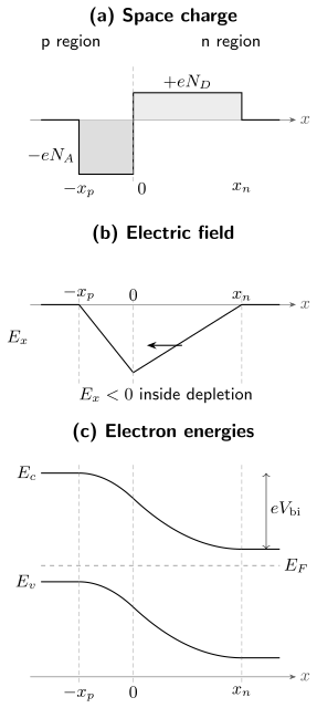
An abrupt junction with , so . The charge areas cancel, the interior field is negative, and both band edges decrease toward the n region while the equilibrium stays flat. The potential and edge curves follow the piecewise depletion solution; panel scales are normalized independently.
What a voltmeter does and does not measure
Section titled “What a voltmeter does and does not measure”is an internal electrostatic difference. It is not an equilibrium two-terminal electromotive force. Metal contacts introduce their own potential changes, and an equilibrium external measurement must include their electrochemical alignment. A dark junction at a single temperature cannot continuously power a load from its built-in field. Illumination, a temperature difference or an external bias supplies additional nonequilibrium physics.
Applied bias, capacitance and injection
Section titled “Applied bias, capacitance and injection”Define the forward terminal voltage as . With ideal contacts and negligible voltage loss in the neutral regions, the depletion drop becomes . Within the same approximation,
Forward bias narrows depletion; reverse bias widens it. Do not extrapolate this square root through . Before a real barrier becomes flat, mobile charge, injection, contact and series-voltage effects can invalidate its assumptions.
The positive n-side depletion sheet charge is , in , and the p-side charge is . With the stated forward-voltage sign, the positive depletion capacitance per area is
For junction area , when fringing is negligible. Capacitance from stored injected carriers, interface traps or quantum confinement is additional physics; a measured capacitance is not automatically .
A numerical electrostatics example
Section titled “A numerical electrostatics example”Use the illustrative silicon-like inputs , , , and . These are specified model inputs, not a parameter fit to a particular sample. Recall that .
The formulas give , , and . The peak field is about and . At , the depletion estimate falls to ; at , it grows to .
Quasi-Fermi levels and the ideal diode limit
Section titled “Quasi-Fermi levels and the ideal diode limit”A biased junction generally has no single equilibrium . If each carrier population has a local thermal distribution at temperature , define electron-energy quasi-Fermi levels by
Their splitting measures departure from equilibrium:
Under ideal injection conditions, the minority densities at the depletion edges are enhanced by . In a long neutral p region, excess electrons decay over ; in the neutral n region, excess holes decay over . For example, for . This exponential solves the steady continuity equation and tends to zero deep in the p region. Its edge diffusion current is in the positive direction. Adding the hole contribution yields
This is the steady, low-injection, diffusion-limited diode result described in MIT’s The pn Junction Diode I (2009). It assumes ideal contacts, long neutral regions, constant minority lifetimes and negligible depletion recombination, tunneling, avalanche and series resistance. The exponential is an injection boundary condition, not a single-particle barrier-transmission probability. Low injection requires the added minority density to remain small relative to the majority density on each side. With the stated nondegenerate boundary values, this means in forward bias. The quasi-Fermi splitting also need not equal everywhere inside an operating device.
Heterojunction offsets need a common energy reference
Section titled “Heterojunction offsets need a common energy reference”A heterojunction adds composition-dependent edge offsets to smooth band bending. Define the local lineup from material A to material B as
These are electronic energies evaluated using one aligned reference, with the specified interface strain and structure. Necessarily,
For positive bulk gaps, the following cases distinguish where electrons and holes prefer to reside. Holes favor the higher valence edge.
| Alignment | Conditions for the stated A/B assignment | Consequence |
|---|---|---|
| Type I, A is the well | , | Both electron and hole confinement favor A. |
| Type II, electrons in A and holes in B | , , | The favored carriers occupy opposite materials with a positive cross-interface gap. |
| Type III, broken gap in this orientation | A conduction edge lies below the other material’s valence edge; charge transfer and electrostatic reconstruction must be considered. |
Reversing A and B changes the signed offset statements. Equalities mark boundaries between these cases.
Separate bulk calculations have arbitrary energy zeros. Their plotted eigenvalues cannot be subtracted to obtain an interface offset. Van de Walle and Martin (1987) distinguish bulk band-edge contributions from the electrostatic lineup across an interface. Interface dipoles, atomic structure and strain can matter. The electron-affinity estimate follows only from an assumed vacuum-level alignment; it is not a universal interface theorem.
Once a lineup is supplied, Quantum Wells develops envelope matching and subband confinement. A discontinuous offset and smooth electrostatic bending are separate inputs to that calculation.
Field-effect control in a metal–oxide–semiconductor structure
Section titled “Field-effect control in a metal–oxide–semiconductor structure”Consider an ideal planar gate, insulating oxide and uniformly doped p-type semiconductor with fully ionized acceptors and nondegenerate bulk carriers. The bulk terminal is the voltage reference, with no separate source-to-body bias. Let , be oxide capacitance per area, and be total semiconductor sheet charge. With negligible oxide leakage and interface traps,
is gate voltage relative to the bulk terminal; accounts for the work-function lineup and any separately modeled fixed-charge shift. The equation divides gate voltage between semiconductor bending and oxide field.
For , both electron-energy edges bend downward at the surface. Holes are depleted and ionized acceptors give
before mobile inversion charge dominates. Define . The equilibrium surface electron density reaches the bulk majority-hole density when . Evaluating the depletion charge there gives the conventional threshold estimate
This electrostatic construction, also developed in MIT’s PN Junction and MOS Electrostatics IV (2009), is a useful strong-inversion criterion, not a thermodynamic phase transition. Beyond threshold, additional gate bias mainly changes mobile electron sheet charge in the usual quasistatic picture. For , holes accumulate instead.
Real capacitance depends on measurement frequency, carrier supply, traps and oxide properties. Confinement subbands, finite density of states and quantum capacitance require the treatment at Two-Dimensional Electron Gases. A capacitor’s equilibrium band bending alone does not determine a transistor’s nonequilibrium channel current.
Quantum confinement becomes important when the conducting layer is narrow enough to resolve subbands; Quantum Wells and Two-Dimensional Electron Gases develop that limit. Interfaces and contacts add further structure, discussed in Device Fabrication Concepts and Transport Measurements.
Exercises
Section titled “Exercises”1. Check equilibrium currents without guessing their signs
Section titled “1. Check equilibrium currents without guessing their signs”In one homogeneous material, differentiate the equilibrium and formulas and show that both drift–diffusion charge currents vanish. Would a constant carrier density also cancel the drift term in a nonzero field?
Solution
Since , one has and . With and , the electron terms are and ; the hole terms are and . Each pair cancels. Constant nonzero density would remove diffusion and leave a drift current within this model, so it is incompatible with this field and thermal equilibrium.
2. Charge, field and reverse-bias scaling
Section titled “2. Charge, field and reverse-bias scaling”For , find . If reverse bias raises the depletion potential drop from to , determine the changes in , peak field, and . Verify the sign of .
Solution
Charge neutrality gives . The width is proportional to , so both widths, the peak field magnitude and double. The capacitance per area halves. Differentiating gives
The field itself remains negative in the depletion region. The larger positive electrostatic drop means a larger fall in electron-energy edges from p to n.
3. Distinguish offset type from gap size
Section titled “3. Distinguish offset type from gap size”For energies in electronvolts, classify these aligned pairs : , and . Check the gap-difference identity in each case.
Solution
The first is type I: , , and . The second is type II with electrons favoring A and holes B: the offsets are and , and . Its cross-interface gap is .
The third is type III since . Each individual material still has a positive gap, and . The offsets are and , giving . Broken alignment does not require either bulk material to have a negative gap.
4. Diagnose injection and surface inversion
Section titled “4. Diagnose injection and surface inversion”First take and find . Then, for an equilibrium p-type semiconductor with , derive the surface potential at which . Explain why these two calculations use different equilibrium assumptions.
Solution
The quasi-Fermi splitting gives . This is a nonequilibrium carrier population; it does not redefine the material’s intrinsic density.
In the equilibrium field-effect calculation, and . Setting gives . Here one equilibrium Fermi level suffices in the semiconductor. The gate changes electrostatic boundary conditions without requiring a steady carrier current through the ideal oxide.
References
Section titled “References”- Massachusetts Institute of Technology. “PN Junction and MOS Electrostatics II.” Lecture 5, 6.012 Microelectronic Devices and Circuits, Spring 2009. MIT OpenCourseWare. Lecture notes.
- Massachusetts Institute of Technology. “PN Junction and MOS Electrostatics IV.” Lecture 7, 6.012 Microelectronic Devices and Circuits, Spring 2009. MIT OpenCourseWare. Lecture notes.
- Massachusetts Institute of Technology. “The pn Junction Diode I: I–V Characteristics.” Lecture 14, 6.012 Microelectronic Devices and Circuits, Spring 2009. MIT OpenCourseWare. Lecture notes.
- Van de Walle, Chris G., and Richard M. Martin. “Theoretical study of band offsets at semiconductor interfaces.” Physical Review B 35, 8154–8165 (1987). doi:10.1103/PhysRevB.35.8154.